WHY CHOOSE ALWYN GLOBAL?

01 Expert Hardware Engineers
A team of highly skilled electrical and electronics engineers with strong expertise in complex PCB architecture, signal integrity, and circuit optimization.
02 Advanced Design Capabilities
Specialized in multilayer, high-speed, high-density, and high aspect ratio PCB designs built for performance, reliability, and scalability.
03 End-to-End Execution
Complete lifecycle support from initial schematic designs and PCB layout through prototyping, functional validation testing, and complete production readiness phases.
04 Industry-Focused Solutions
Proven experience delivering high-tier PCB sub-systems for Semiconductor, Automotive, Telecom, Industrial Automation, IoT, and Consumer Electronic sectors.
05 Cutting-Edge EDA Suites
Access to industry-leading design and multi-tier simulation platforms, enabling faster, accurate prototype validation and optimized hardware profiles.
06 Quality & Accelerated Turn
Strong operational focus on design manufacturability (DFM rules), international testing criteria, and rigid on-time scheduling protocols.
07 Production Ecosystem
Seamless collaboration with certified global fabrication, assembly foundry facilities, and manufacturing partners for efficient rapid-prototype runs.
08 Customer-Centric Support
Dedicated direct technical engineering liaisons, completely transparent operational milestone reporting, and customized layout adjustments tailored to criteria.
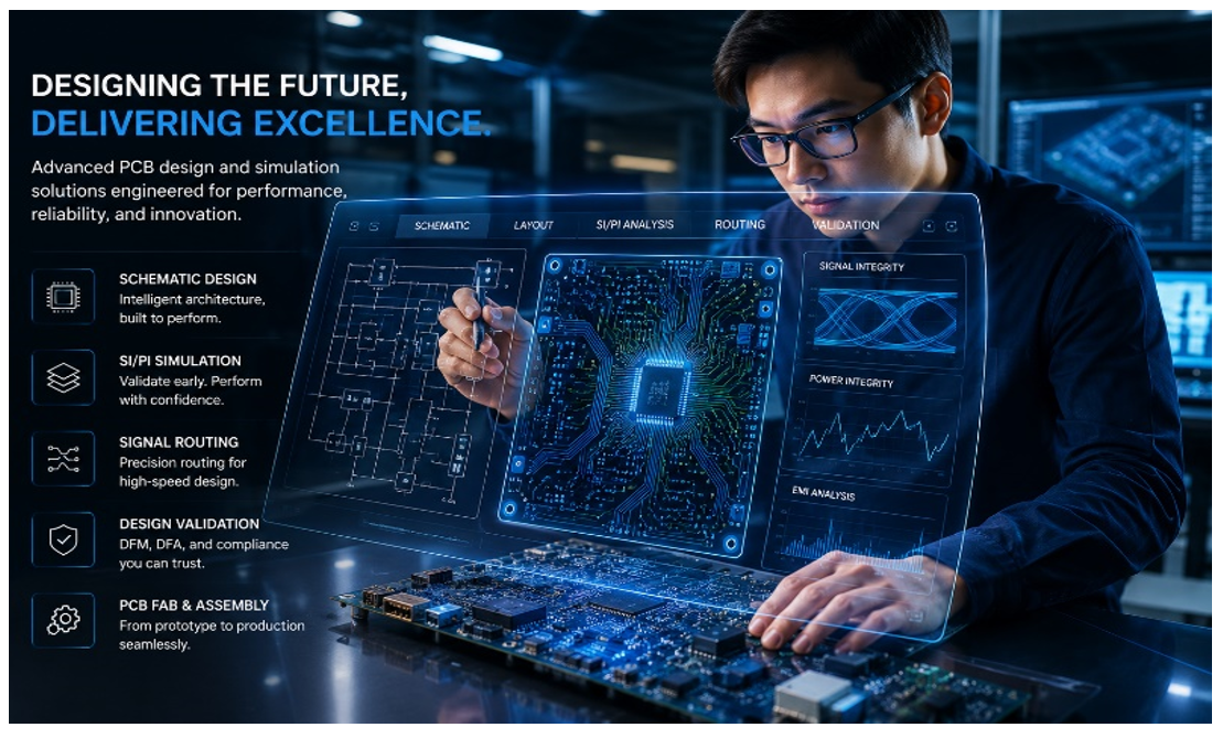
HARDWARE DESIGN AREAS OF EXPERTISE
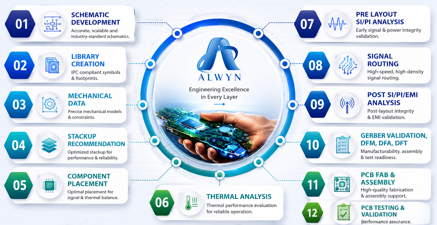
Schematic Development
Accurate, scalable, and industry-standard schematics calculated for production efficiency.
Library Creation
IPC compliant schematic symbols & footprint generation for seamless manufacturing matching.
Mechanical Data
Precise mechanical models, structural outline shapes, and integration constraints checks.
Stackup Recommendation
Optimized layer stackup calculations tailored explicitly for maximum performance & reliability.
Component Placement
Optimal component distribution for enhanced signal pathways and stable thermal balance maps.
Thermal Analysis
Deep thermal performance evaluations under heavy processing load layouts for reliable system operation.
Pre Layout SI/PI Analysis
Early signal integrity & power integrity validation passes running ahead of copper layout routing.
Signal Routing
High-speed, ultra-high-density signal trace routing preserving clean wave propagation shapes.
Post SI/PI/EMI Analysis
Post-layout trace integrity matrices, cross-talk reduction loops, and strict EMI validation safety checks.
Gerber Validation
Deep validation testing covering DFM, DFA, and DFT metrics for total manufacturing readiness.
PCB Fab & Assembly
High-quality fabrication management and ongoing assembly line optimization support services.
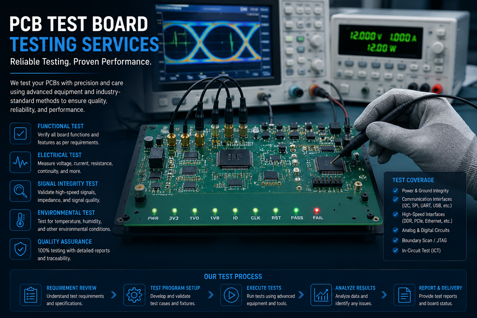
PCB Testing & Validation
Rigorous final hardware bench testing for absolute performance assurance across systems.
TECHNICAL AREAS OF EXPERTISE
Semiconductor Test Board Design
Empowering semiconductor companies with fast, reliable, and scalable ATE PCB design solutions tailored for today's dynamic product development environment.
- Focused Expertise in ATE PCB Design
- Trusted by Industry Innovators
- Integrated Engineering Approach
- Quality-Driven Execution
- Rapid Turnaround and Scalability
- Optimized for Cost and Performance
Your Agile Engineering Partner for Semiconductor Test Solutions
ATE Test Board – Our Design Services
- Load boards (LB), Handler Interface Board (HIB), DUT Interface Board (DIB)
- Probe cards (Vertical / Cantilever), Spider cards, Probe Interface Board (PIB), Flexible PCB boards.
- Device Characterization Boards
- Burn in Boards, HAST, ESD, Latch-up Boards
Board Design Experience
- RF, Analog, High-Speed Digital, Mixed Signal, and Power Management devices
- High Voltage and High Current devices
- HDI Stackup
- Experience in handling PCB materials like Nelco Meteorwave, Rogers, and Megtron series
- Using inventive measures to deliver custom PCB board design
System Board Design
- As a leading PCB design and hardware engineering partner, we develop high-performance system and evaluation boards that enable customers to validate product functionality before full-scale manufacturing.
- Our engineering team delivers application board development backed by deep expertise in High-Speed Processors, Analog, Mixed-Signal, and RF technologies.
- We provide FPGA emulation, logic development, and porting services, ensuring seamless product readiness for certification requirements including RoHS, EMI, and EMC compliance.
- Leveraging innovation-driven engineering, we have also developed our in-house MAGIK-2 Platform Evaluation Kit to accelerate hardware validation and product development cycles.
Our Value-Added Engineering Services
- We deliver advanced hardware design solutions for next-generation technologies including HSIO, 5G, mmWave, PAM4, Silicon Photonics, High-Power Systems, 100+ GB/s Data Applications, and High-Reliability (Hi-Rel) Electronics.
- Our engineering expertise spans complex PCB architectures across diverse materials, layer densities, and component-intensive designs, enabling high-performance and manufacturing-ready hardware solutions.
- We proudly partner with global leaders across Semiconductor, Defense, Automotive, Medical Devices, Data & Telecom, IoT, and Consumer Electronics industries, supporting innovation from concept to production.
Boards We Support
Our engineering team delivers expertise across a wide range of complex PCB architectures designed for high-performance and mission-critical applications.
Supported Board Types:
- RF & Microwave Application Boards
- High-Performance Motherboards
- High-Speed Backplanes
- Sensor Interface Boards
- High-Reliability (Hi-Rel) Boards
- Evaluation & Development Modules
- Bench Testing Boards
- Sub-System Boards
- Daughter Cards
- New Product Introduction (NPI) Boards
- Avionics & Aerospace Boards
PCB Component Library Services
- Ensure seamless design release and future design revisions with comprehensive product documentation, including detailed component specifications, footprints, and complete design data.
- Supported by a dedicated component library team, we create accurate schematic symbols and PCB footprints from manufacturer datasheets in compliance with IPC standards (IPC-7351), leveraging an extensive validated library database to ensure consistency, manufacturability, and reliability.
Our Library Services
- Component Library Development, Administration, and Verification
- Library Migration – Legacy to Latest designs with add-on services such as BOM cleaning, Component Obsolescence identification, finding alternates, etc.
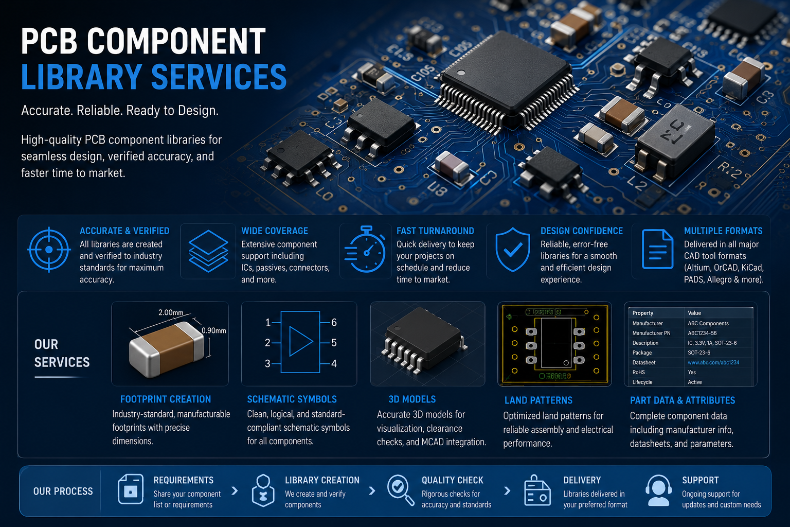
Benefits & Highlights
- Footprints developed in strict adherence to IPC-7351 standards
- An innovative parts review process ensures zero defect symbols and footprints
- Dedicated Library development and management team ensure quick turnaround service
- Library documentation conforms to the engineering rules established within IPC-7351
- Automation scripts deployed to ensure quality and reduce cycle time
- In-house developed Library QMS for process standardization
PCB Simulation Services
- Validate PCB performance and signal integrity through advanced analysis techniques that identify potential issues before fabrication.
- Go beyond post-layout verification with pre-layout design evaluation, enabling informed architectural decisions and optimized board performance from the outset.
- Leverage simulation-driven design using accurate models, rule-based validation, and virtual prototyping to ensure reliable operation under real-world conditions.
- Mitigate design risks early through rapid performance analysis and targeted simulations, reducing layout iterations, development time, and overall project costs.
Simulation Tools Expertise
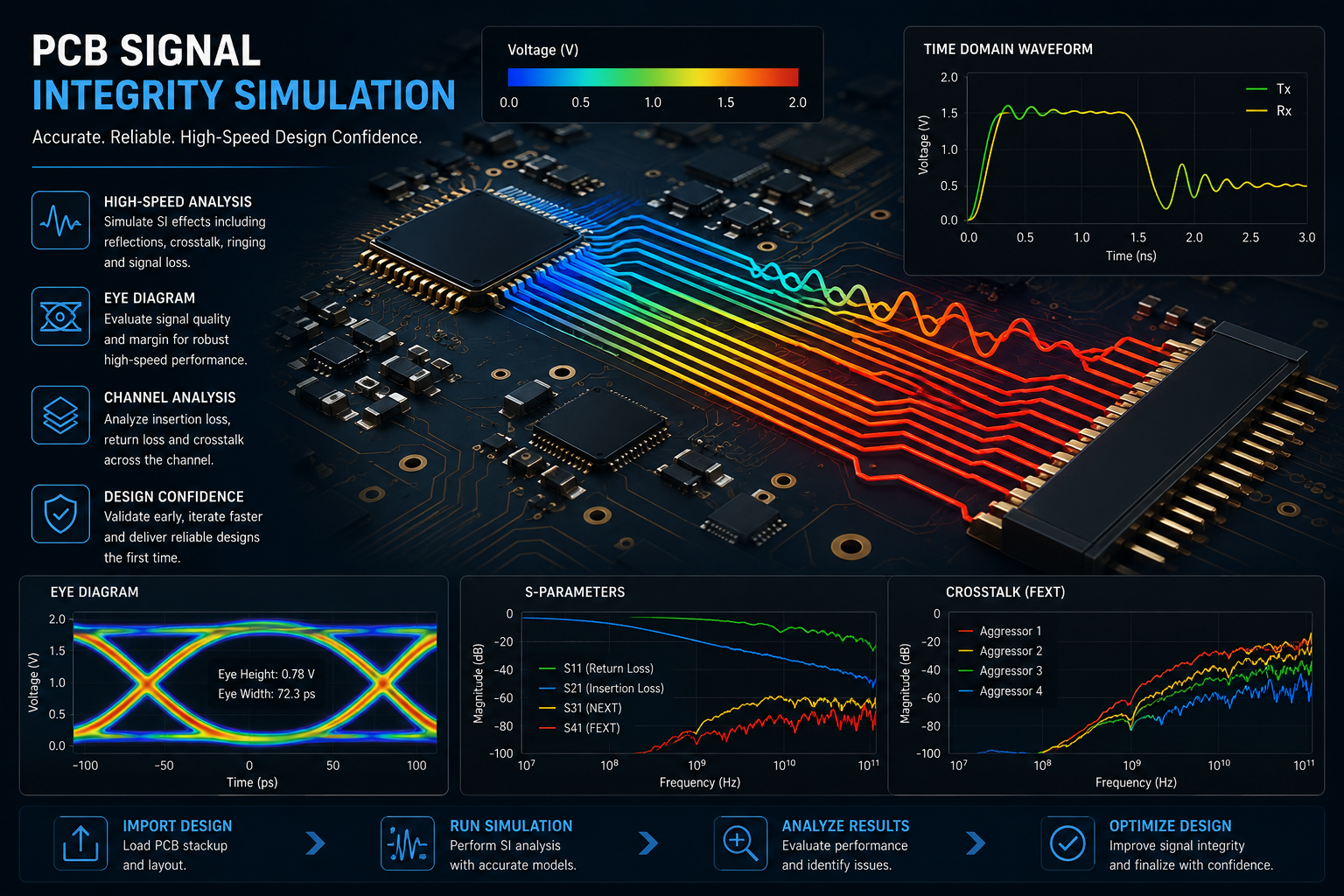
Our Simulation Services Matrix
- High-Speed Channel Simulation – Optimize signal quality and timing performance for high-speed interfaces through comprehensive channel analysis and validation.
- Time-Domain Waveform Simulation – Analyze transient behavior and waveform integrity to ensure reliable signal transmission under real-world operating conditions.
- Power Integrity (PI) Simulation – Evaluate power delivery networks to minimize voltage fluctuations, noise, and power-related performance issues.
- Thermal Simulation – Predict heat distribution and thermal behavior to enhance reliability, performance, and product lifespan.
- Crosstalk Analysis & Simulation – Identify and mitigate unwanted electromagnetic coupling between signals to maintain data integrity.
- EMI / Radiated Emissions Simulation – Assess electromagnetic emissions early in the design cycle to improve EMC compliance and reduce certification risks.
- Parasitic RLC Extraction & Simulation – Model real-world parasitic resistance, inductance, and capacitance effects for accurate performance prediction and design optimization.
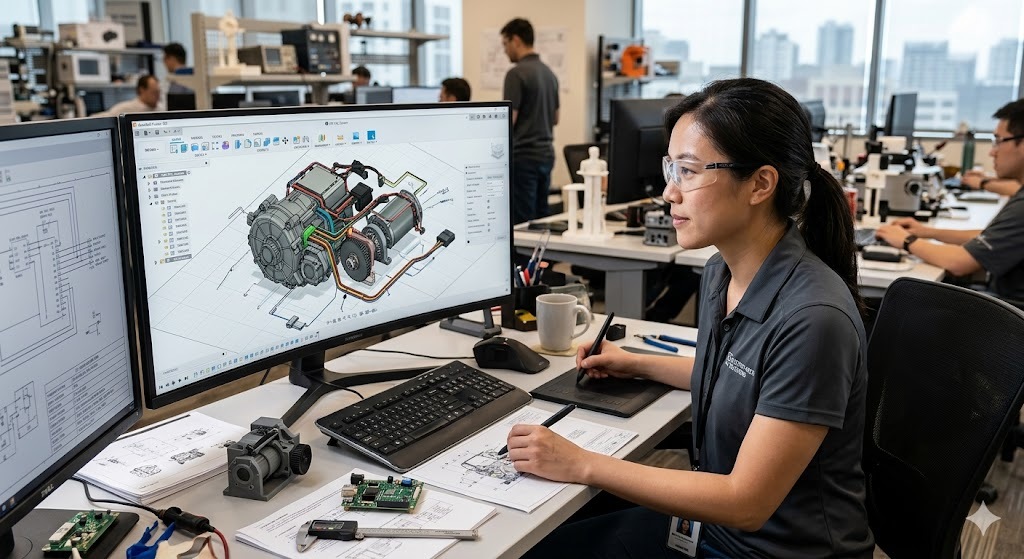
Mechanical Engineering
- Serving diverse industries with end-to-end mechanical and electro-mechanical engineering solutions, continuously expanding our capabilities to address evolving product development challenges.
- Design and develop test fixtures, customized test cells, enclosures, and complete electro-mechanical systems while enabling rapid validation of design changes before physical prototyping.
- Partner with our experienced engineering team to transform complex electro-mechanical concepts into reliable, manufacturable, and production-ready solutions.
Our Mechanical Engineering Services
- Enclosure Design
- Product/System Architecture
- Shock/Vibration Simulation
- Thermal Simulation and Analysis
- Material and Comp. Selection
- Reverse Engineering with CMM technology, Laser scanning
- Product Specifications drafting
- 3D Rendering and Prototype Design