Our Competence
Advancing the Art of Package Engineering
Delivering advanced IC package designs that address complex customer requirements while ensuring superior performance and long-term reliability.
Optimizing bump placement, BGA pin assignments, and critical routing to achieve superior Signal Integrity (SI), Power Integrity (PI), thermal performance, and manufacturability in compliance with Design for Manufacturing (DFM) guidelines.
Delivering advanced IC package designs that address complex customer requirements while ensuring superior performance and long-term reliability.
Supported Solutions
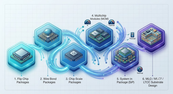
Advanced Semiconductor Packaging Technologies
Modern silicon demands flexible, reliable, and high-density packaging architectures to bridge the gap between complex die logic and substrate manufacturing layouts. Our engineering capabilities accommodate highly sophisticated form-factors optimized for high-bandwidth performance, thermal stability, and maximum structural integrity.
✓
Custom Substrate Routing: Optimized multi-layer design rules ensuring pristine signal transmission pathways.
✓
Thermal & Structural Compliance: Precision mapping to combat extreme thermal dissipation vectors.
Execution Framework
Our Delivery Methodology
A structured, multi-tier architectural layout driven by rigorous cross-collaboration and engineering verification.
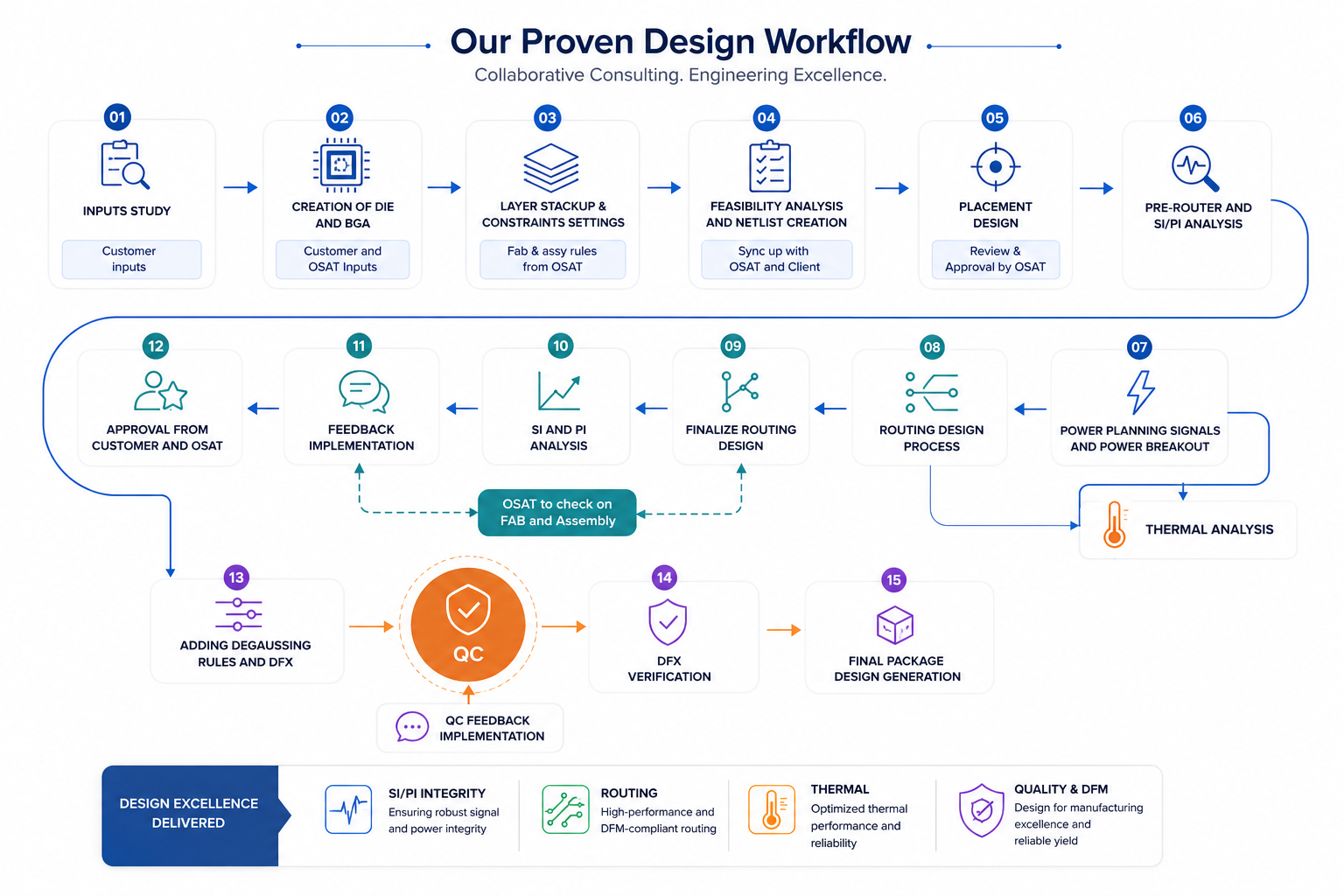
01
Inputs Study
Comprehensive analysis of custom core user and design parameters.
02
Creation of Die and BGA
Detailed alignment mapping utilizing Customer and OSAT specifications.
03
Layer Stackup & Constraints
Integration of critical fabrication and assembly routing rules straight from OSAT.
04
Feasibility & Netlist Creation
Real-time collaborative synchronizations across OSAT partners and client engineering teams.
05
Placement Design
Rigorous physical layout placement culminating in final Review & Approval by OSAT.
06
Pre-Router & SI/PI Analysis
Advanced simulations optimizing comprehensive Signal Integrity and Power Integrity checks.