
Our Competence
Advancing the Art of Package Engineering

Delivering advanced IC package designs that address complex customer requirements while ensuring superior performance and long-term reliability.

Optimizing bump placement, BGA pin assignments, and critical routing to achieve superior Signal Integrity (SI), Power Integrity (PI), thermal performance, and manufacturability in compliance with Design for Manufacturing (DFM) guidelines.

Delivering advanced IC package designs that address complex customer requirements while ensuring superior performance and long-term reliability.
Supported Solutions
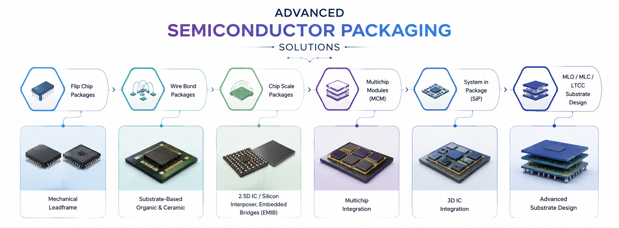
Advanced Semiconductor Packaging Technologies
Modern silicon demands flexible, reliable, and high-density packaging architectures to bridge the gap between complex die logic and substrate manufacturing layouts. Our engineering capabilities accommodate highly sophisticated form-factors optimized for high-bandwidth performance, thermal stability, and maximum structural integrity.
✓
Custom Substrate Routing: Optimized multi-layer design rules ensuring pristine signal transmission pathways.
✓
Thermal & Structural Compliance: Precision mapping to combat extreme thermal dissipation vectors.
Execution Framework
Our Delivery Methodology
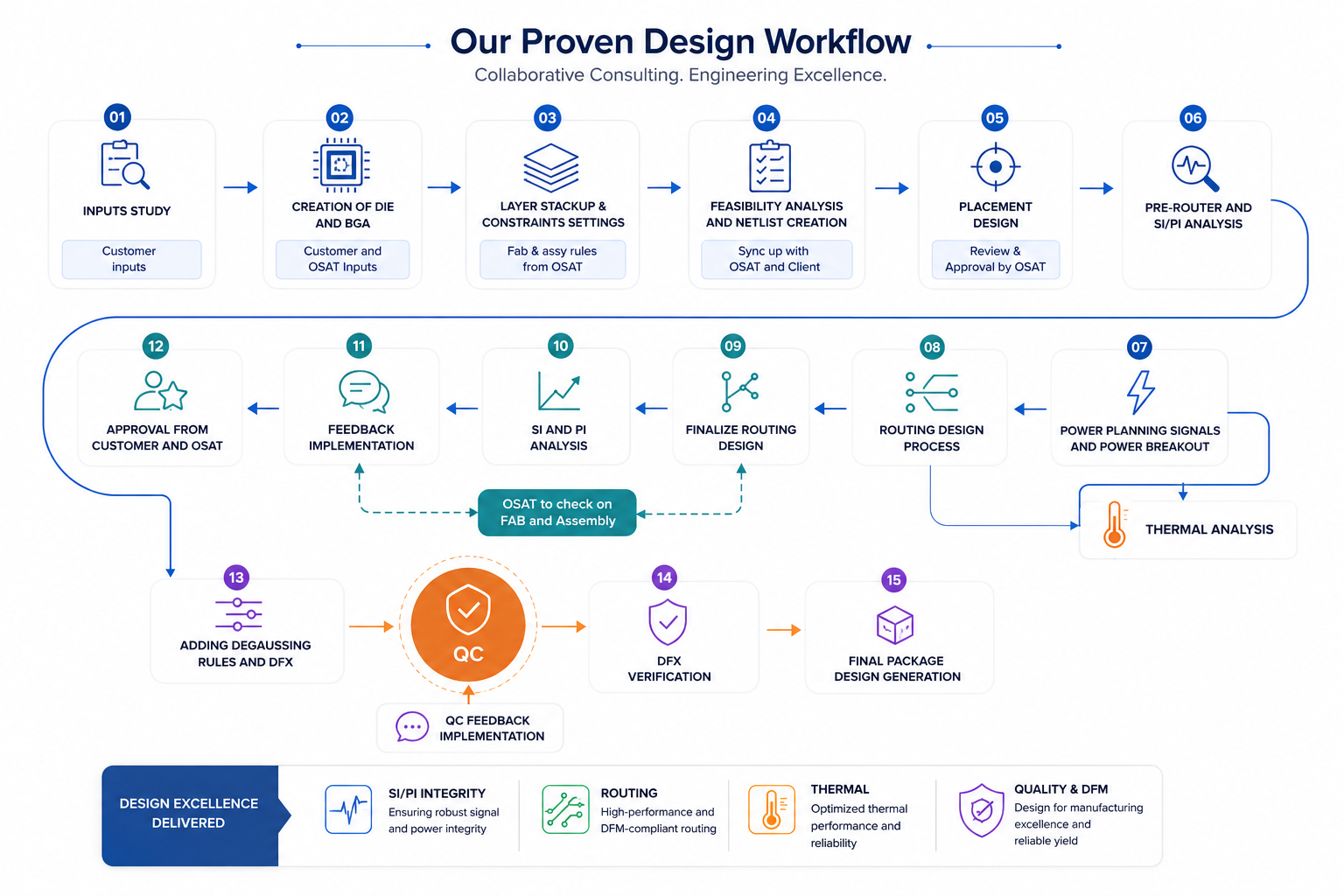
A structured, multi-tier architectural layout driven by rigorous cross-collaboration and engineering verification.
01
Inputs Study
Understand customer requirements, package specifications, and design objectives.
Review electrical, mechanical, thermal, and reliability requirements before design begins.
02
Creation of Die and BGA
Create the die outline and Ball Grid Array (BGA) layout based on customer specifications.
Define die dimensions, bump locations, and ball assignments for the package.
03
Layer Stackup & Constraints Settings
Define the substrate layer stackup and routing structure.
Apply fabrication, assembly, spacing, and routing rules provided by the OSAT.
04
Feasibility Analysis & Netlist Creation
Verify the design feasibility by checking connectivity and package constraints.
Generate and validate the netlist to ensure correct signal mapping.
05
Placement Design
Place the die and package components for optimal routing and performance.
Review the placement with the OSAT to ensure manufacturability.
06
Pre-Router and SI/PI Analysis
Perform preliminary routing to evaluate signal paths.
Run initial Signal Integrity (SI) and Power Integrity (PI) analysis to identify potential issues early.
07
Power Planning Signals and Power Breakout
Design efficient power and ground distribution throughout the package.
Route power breakouts from the die while minimizing voltage drop and noise.
Analysis
Thermal Analysis
Analyze heat distribution and identify potential thermal hotspots.
Optimize the package design to improve heat dissipation and reliability.
08
Routing Design Process
Complete signal, power, and high-speed routing according to design constraints.
Ensure impedance control, length matching, and routing quality for reliable performance.
09
Finalize Routing Design
Review and optimize the completed routing for electrical and manufacturing compliance.
Resolve design rule violations and prepare the layout for verification.
OSAT Check
OSAT Check on FAB and Assembly
Validate the design with the OSAT for fabrication and assembly compatibility.
Incorporate recommendations to improve manufacturing yield and reliability.
10
SI and PI Analysis
Perform detailed Signal Integrity and Power Integrity simulations on the final design.
Verify signal quality, power delivery, and overall electrical performance.
11
Feedback Implementation
Implement design changes based on customer, OSAT, and simulation feedback.
Update the layout and revalidate the design where necessary.
12
Approval from Customer and OSAT
Submit the completed design for customer and OSAT review.
Obtain final approval before releasing the design for manufacturing.
13
Adding Degassing Rules and DFX
Apply degassing and Design for Excellence (DFX) guidelines to improve manufacturability.
Ensure the design meets DFM, DFA, and reliability requirements.
QC Gate
QC (Quality Check)
Perform comprehensive quality checks to verify design accuracy and compliance.
Identify and resolve any remaining issues before final release.
QC Review
QC Feedback Implementation
Address all observations raised during the quality review process.
Implement corrections and confirm that the design meets quality standards.
14
DFX Verification
Verify that the design complies with manufacturing, assembly, and test requirements.
Ensure the package is optimized for production, yield, and long-term reliability.
15
Final Package Design Generation
Generate all final manufacturing deliverables, including layout and fabrication files.
Release the complete package design database for production and assembly.